So it is now our job to choose these values such that we get the desired logic functionality we want!
Notice though that usually (usually and ) are given values that we have to work around, so then usually the voltages are out of our control. Recall from Modules 1 & 2 - NMOS Review#6.1 Ideal Logic Gates that was usually .
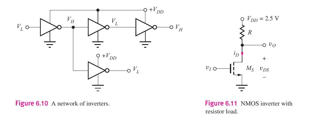
We first do logic design by making a simple logic inverter:
We'll explore the intricacies of this NMOS inverter with resistor load now.
Looking at Figure 6.11 seen [[Pasted image 20240117112307.png]], we use a resistor load to "pull" the output up towards the power supply . So when the MOSFET is "off" then no current flows, so , as we wanted. And when the MOSFET is "on" then as desired too.
We need to choose values for and of switching transistor such that we can meet the design specifications, letting us choose and the total power dissipation for the gate. We summarize everything below:
NMOS Inverter
When :
And when :
So therefore the power supply voltage sets what a logic high is. Further, for we require that .
Design
For something like a good rule of thumb is to have .
6.5.2: Design of the Ratio for
will come from our chosen value for . Say we have , so as the design note above mentions, then :
Choosing
Say . Say we're given . The current is determined by the power dissipation of the NMOS gate when . Say . Then we know that so then:
Thus, when our then we have . We use the triode drain current since , while , so which gives rise to the triode behavior. Thus:
Plugging in:
Thus:
6.5.3: Load Resistor Design
How do we choose ? We choose it based on when , which has:
Choosing
Redesign the logic gate designed in Example 1 to operate at a power of while maintaining . Really, is getting doubled, which would double . Thus, we expect:
Similarly, is inversely proportional to so then gets halved to .
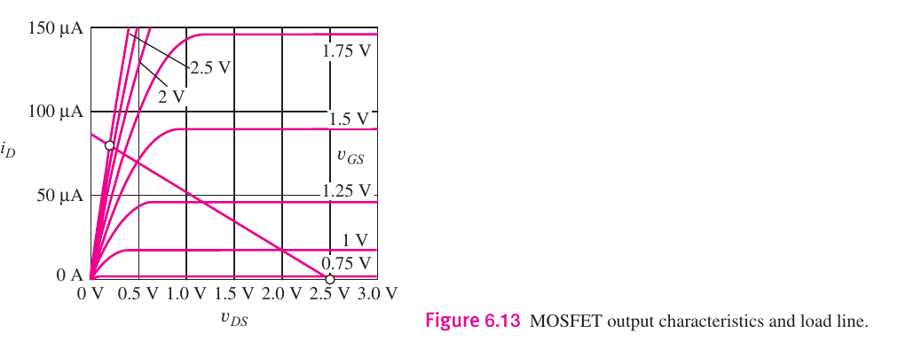
6.5.4: Load-Line Visualization
We'll look at the IV characteristic using:
When we are in CO, we have so then . When we're in the triode region then we have so then . But we must have some switch in operating modes between and . We can draw the load line to visualize when this change happens:
Here, we connect the two points described above to see where our Q-point is. In this case, the Q-point is the left point, where the slope's inverse indicates the MOSFETs load resistance.
Consult [[microelectronic-circuit-design-4th-edition-jaeger1.pdf#pages=301]] for a design process using this idea.
6.5.5: On-Resistance of the Switching Device
We can generalize this process, as we really only care when or , using the as a factor here using a voltage divider:
So for to be small, we require that . This whole idea gives rise to the idea of ratioed logic, where we design based on this ratio, rather than the values themselves.
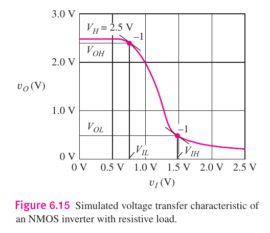
6.5.6: Noise Margin Analysis
Using our designs above, we can simulate or do the math ourselves and get an IV plot:
of which now we can find the points which give the points.
6.5.7: Calculating and
We do an example of this now. Consider again:
When we have as small () and is large (relatively speaking, since ). Thus, we are likely in the saturation region:
Substituting this in gives:
We want to find the slope at this point to get the -1 slope points:
We know these points have -1 slope so:
where plugging this back in as from our equation:
We usually note that has units of voltage, so it's the ratio of the transistor's transconductance parameter (say that 10 times fast).
6.5.8: Calculating and
Likewise, we do the same for the other 2 parameters. When then is large and is small so we are in the triode region. Thus:
We substitute in back into our generic equation to get:
We can do some rearranging to get:
We solve for and set the derivative of to -1 for to get:
I'd recommend not doing it this way and instead using the equations defined in terms of and finding those instead using the above equations.
6.5.9: Load Resistor Problems
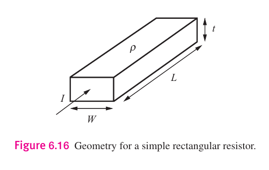
Consider a rectangular block of semiconductor material:
The resistance is given by:
For say a resistor like the we usually we, we require the ratio to be:
So if the was some minimum line width of , then . The area would be while the transistor itself is only which wouldn't be acceptable.
6.6: Transistor Alternatives to the Load Resistor
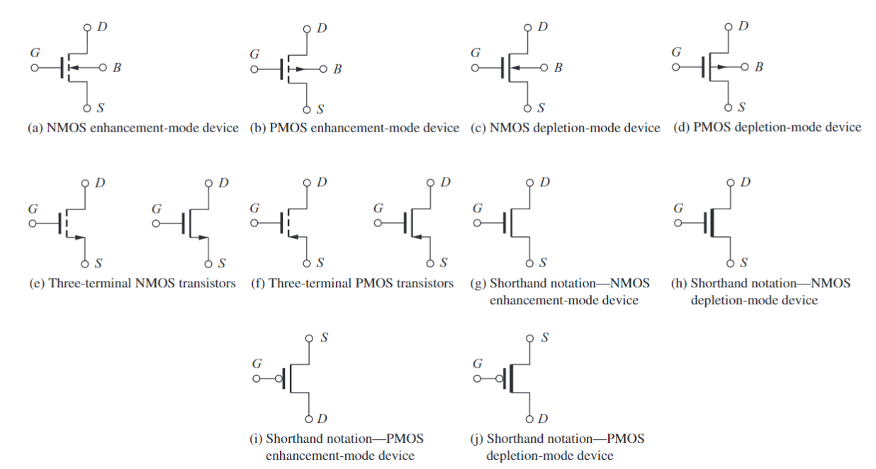
The in our previous calculations just sucked! How about we remove it? Change with some new NMOS transistor .
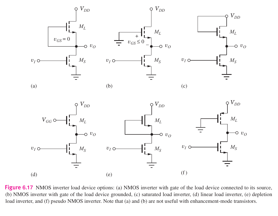
(a) and (b) are always either turned always off or on. But (c-e) have properties that'll be interesting to us.
6.6.1: The NMOS Saturated Load Inverter
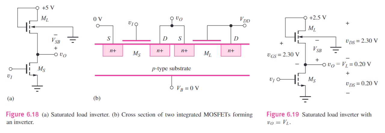
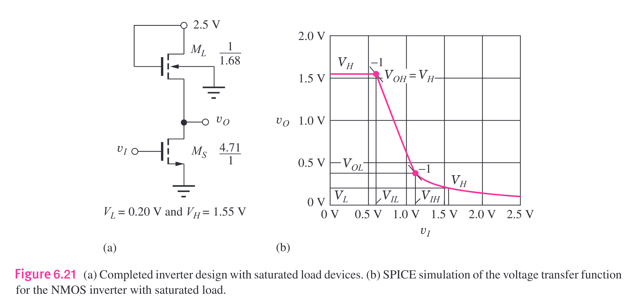
First consider (c). Here in . We refer to this as a saturated load inverter.
Notice:
The -type substrate is common between the .
We have (ie: connect it to ground), so then for , but for we have . This will affect for both so then we denote each separately as and .
Consider for our cases that and and . We know that has to operate in the saturation region (as so then for ), so then:
We know that when then and . Other values are in Figure 6.19 above. But we need to get first, which is given by:
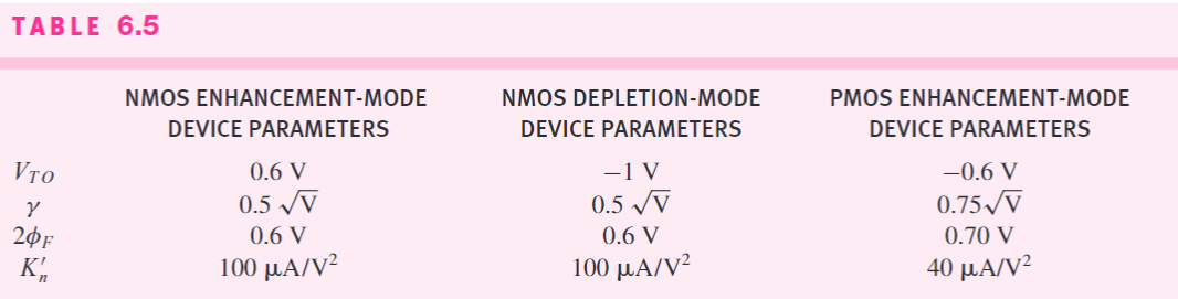
We usually are just given these values from a table, so we'll use:
Cool! So then:
Now solve for in the current equation above:
So now the has to be bigger than , but we still use the larger side as the measure of size. With that, then the gate area is .
Calculation of
We'll find that the value of sadly. Consider the following circuit:
Consider , so then is turned off. But will approach so we'd reach rather than . But with body effect we consider the entirety of which is lower than .
Really, we use the same equation as before, so for instance:
where as per usual.
Calculation of
is just:
where we do some solving via using a calculator to find the intersection for .
Calculation of
For the switching transistor calculating the ratio is via determining the region of operation based on given design values. For triode:
Notice here as it suddenly gives to a negative slope.
6.6.2: NMOS Inverter w/ A Linear Load Device
Consider (d) now. The gate is connected to a , which is normally chosen to be at least one threshold voltage greater than the supply voltage :
Again, like the previous analysis, consider as equal to , as:
We can check the region of operation by seeing when :
but since then always we are always in the triode region. As before we can solve for the ratios for both MOSFETs. We know that . We can use a graph to estimate
6.6.3: NMOS Inverter w/ Depletion-Mode Load
Consider (a) now. Notice that since is always negative, as the typically is negative for depletion-mode NMOSFETs (not enhancement mode), so then we are usually in saturation via:
so we require for that state that .
Design of ratios for .
Assume , and . When then . So the MOS operates in saturation, then:
if there's body effect we account for that in our calculation: